Science is key for product quality and customer service
By Dr. Christophe Gras | July 23, 2018
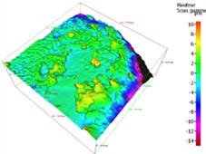
Quality and service to customers are C&K’s primary concern which is why we are so committed to improving our product quality processes. Throughout the production, comprehensive quality checks using a series of optical observations tools from macro- to micro (see Figure 1) alongside a variety of equipment that measures specific variables, including a low-load microhardness tester, X-ray fluorescence (XRF) electrodeposit thickness measurement suite, compression/traction testing rigs, lifetests in different environments and electrical properties quantification.
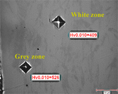
Figure 1: Optical cross-section of stainless steel band AISI301 shaped as a dome and low-load Vickers microhardeness measurements (Hv) – two phases coexist, one harder than the other
C&K is also committed to supporting our customers during product development towards final usage. Complicated issues related to product integration (e.g. soldering) require in-line investigations with state of the art analytical tools. For example, soldering flux penetration can be characterized using Infrared (IR) microscopy since it provides local structural information on organic-based materials/contaminations.
Corrosion is another important topic our clients often face which is why C&K is able to perform tests in high-stress environments – including salt spray tests, SO2 and 4 gases – that unveil insights into our products’ behavior. We use in-house optical 3D topographic representations (see Figure 2) and electron microscopy (SEM) coupled to local composition estimation (EDX) technology to fuel our own R&D development so we can pass that knowledge along to our customers.
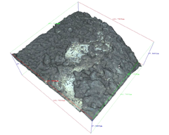
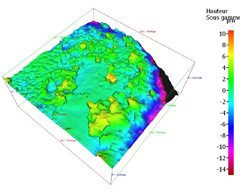
Figure 2: 3D Optical image of highly corroded silver surface
Corrosion resistance improvement starts with complete control of the electrodeposition process that should include the microstructure of the plated layers. Imaging-based Field Ion Beam (FIB) sections have been recognized as a useful tool (see Figure 3), especially when it is coupled with standard topographic observations and X-Ray fluorescence (XRF) thickness estimations.
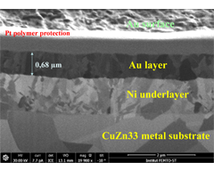
Figure 3: FIB section ionic imaging mode of Au/Ni/CuZn33 plating sequence
C&K is continuously working on new concepts and always looks for the best analytical tools associated with common issues such as silver tarnishing in electrical contacts. C&K is working to define the best post-treatment process that can be applied to extend switches’ performances and shelf-life. Rather than accepting limitations from our providers, C&K pushes further and deploys X-ray Photoelectron Spectroscopy (XPS) surface analysis to identify the first nanometer of the metal surface and define the structure of the organic post-treatment layer to battle tarnish.
Finally, non-destructive characterization methods such as computerized X-ray microtomography (µCT) have emerged as a powerful tool to understand the dynamic of the newly developed products. In addition, 3D high-resolution metrology and direct comparison of the final assembly versus CAD files becomes possible; these new virtual concepts can be tested and design-optimized based on 3D data, making faster and more accurate prototyping possible. Figure 4 displays a 3D reconstruction of the metal parts from an ATS switch, including fixed and moveable parts surrounded by the external cage that holds the product together.
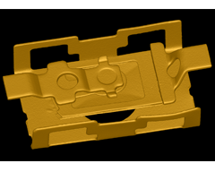
Figure 4: Metal parts and internal contacts from an ATS switch – 3D reconstruction from µCT analysis
